| |
RESEARCH:
S-TEK
research and development center is responsible for all the technology research and development
for the company. The current main research areas include
the design of high-frequency integrated circuits, microelectronic
device model and the related compound semiconductor materials and
devices, and process technology development.
 Personnel and team : with about 20 R & D personnel, five of
them with develop experience in large international companies.
Personnel and team : with about 20 R & D personnel, five of
them with develop experience in large international companies.
Technical resources and research capabilities : The company
owns the major IPs for the products developed.
Development platform and experimental conditions : With strong collaboration with world-class chip manufacturers. With
access to the most advanced process technology in GaAs, including
0.15-micron GaAs PHEMT processe.
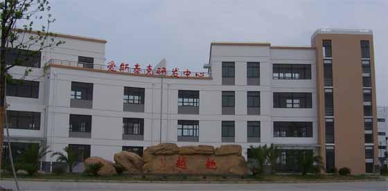
R & D center office : With a R & D center of a total area of 2,000 square meters.
Research and development achievements:
 In
the high-frequency IC design such as GaAs ICs, S-TEK offers several key products including PAs, LNA, etc. In
the high-frequency IC design such as GaAs ICs, S-TEK offers several key products including PAs, LNA, etc.
Silicon germanium and Si RF
CMOS technology
development: IC design based on 0.18um SiGe BiCMOS, and Si RF SOC
based on 0.13um RFCMOS..
Nano-technology

|
|